Micrel
MICRF405
April 2006
27
M9999-041906
(408) 955-1690
Modulation
Adr
Data
A6..A0
D7
D6
D5
D4
D3
D2
D1
D0
0001011 LowBatt_en=1 Freq_Band1=0 Freq_Band0=1 VCO_freq2=0 VCO_freq1=1
VCO_freq0=1 Modulation1=1 Modulation0=0
0001110
Mod_I4=0
Mod_I3=1
Mod_I2=0
Mod_I1=0
Mod_I0=1
Mod_A2=0
Mod_A1=1
Mod_A0=1
0001111 VCO_Fr_Chk=0 VCO_Fr_Auto=0
FSKn2=1
FSKn1=0
FSKn0=0
Mod_F2=1
Mod_F1=0
Mod_F0=0
0010000 MOD_TEST1=0 Prescaler_Sel=0 FSKClk_K5=1 FSKClk_K4=1 FSKClk_K3=0 FSKClk_K2=1 FSKClk_K1=0 FSKClk_K0=0
0010001 ASK_PN_en=0
ASK_EN=0
ASKshape2=1 ASKshape1=1 ASKshape0=1
ASK2=1
ASK1=1
ASK0=1
0010010
ASKn1=1
ASKn0=0
ASKClk_K5=1 ASKClk_K4=1 ASKClk_K3=0 ASKClk_K2=1 ASKClk_K1=0 ASKClk_K0=0
The frequency modulation can be done in three
different ways with the MICRF405, either by closed-,
open loop VCO modulation or by modulation with
the internal dividers. Amplitude modulation can also
be done in two different ways, either ASK/OOK or
Spread Spectrum ASK". All these different types of
modulation is selected by Modulation1-0 and
ASK_en (See chapter bit description for details).
Closed loop VCO modulation (Modulation[1:0]=0),
the modulation is applied directly to the VCO. The
PLL will see the modulation as a frequency error and
try to tune the VCO back to carrier. The PLL
bandwidth therefore, needs to be sufficiently low
enough not to cancel the modulation (at least 20
times lower than the slowest variation of the
modulation). Also, the modulation needs to be DC-
free, usually by encoding the data by a DC-free code
such as Manchester or 3b4b. In most cases, an
external PLL loop filter must be used to fulfill the
demand for low bandwidth. Please see the
Modulator section for details on deviation and
shaping.
Open Loop VCO Modulation (Modulation[1:0]=1),
modulation is applied directly to the VCO. The VCO
is now left free-running. The varactor voltage will
now be stored on a large external capacitor
connected to the VARIN pin and the PLL is disabled
during the modulation. With the PLL disabled, the
modulation will not be canceled and the modulated
data signal may include DC-components. The
switching between PLL active and disabled is done
automatically by checking the DATAIN pin. If it is tri-
stated the PLL is active, and if it is either high or low
or transitioning between high or low the PLL is then
disabled and the data on the DATAIN pin is
transmitted. When data is transferred through the
SPI the PLL is disabled during the transmission of a
packet, while enabled else. In this mode, the PLL
bandwidth can be fairly high as it is disabled during
transmission. However, due to the large external
capacitor, C3 in Figure 11b), the bandwidth is limited
due to the pole created by this capacitor. Both
internal with 56? phase margin and external filters
are suitable. A high quality capacitor of 10-47nF
(COG type) should be connected on pin VARIN-to-
ground to ensure minimum frequency drift due to
leakage and frequency drift caused by the capacitor
dielectric relaxation phenomenon (25kHz offset after
50ms). For deviation and shaping, please see the
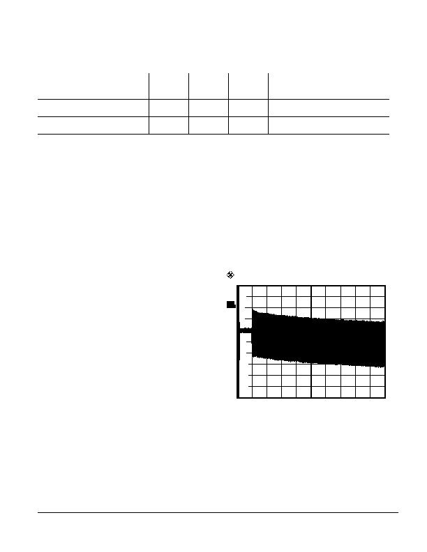
Modulator section. The frequency drift (Hz/ms) over
temperature due to leakage is shown in Figure 12
with a 33nF COG external capacitor.
Figure 13 shows the frequency drift in open loop
VCO modulation due to capacitor dielectric
relaxation. The drift is around 40kHz during a time
period of 50ms. Of the 40kHz drift, 5-10kHz is due to
an initial offset caused by the modulator itself.
tt 30 dB
*
1 AP
CLRWR
A
IFB 10 MHz
TRG
Ref 0 Hz
Center 915.00004 MHz
10 ms/
QT 100 ms
-240k
-200k
-160k
-120k
-80k
-40k
0
40k
80k
120k
160k
Date: 11.JAN.2006 10:10:03
Figure 12. Frequency Drift Due to Capacitor Dielectric
Relaxation at 915MHz.
发布紧急采购,3分钟左右您将得到回复。
相关PDF资料
MTX-102-433DR-B
MODULE TRANSMITTER 433MHZ 18DIP
MTX-103-915DR-B
MODULE TRANSMITTER 915MHZ 18DIP
MTX-405-433DR-B
MODULE TRANSMITTER 433MHZ 24DIP
N50P105
IC MODULE MINI JOYSTICK SMD
OCB350L187Z
BOARD CALIBR CIRCUIT OPB350L187
OMB.242.08F21
OMNI OUTDOOR ANTENNA
OMNILOG90200
ANTENNA ISOTRP 700MHZ-2.5GHZ RAD
OPR5011
COMPARATOR OPTICAL 3 CHAN SMD
相关代理商/技术参数
MICRF405YML-TR
功能描述:RF Transmitter ASK, FSK 290MHz ~ 980MHz 10dBm 200kbps PCB, Surface Mount Antenna 24-VFQFN Exposed Pad, 24-MLF? 制造商:microchip technology 系列:- 包装:剪切带(CT) 零件状态:停产 频率:290MHz ~ 980MHz 应用:ISM 调制或协议:ASK,FSK 数据速率(最大值):200kbps 功率 - 输出:10dBm 电流 - 传输:18mA 数据接口:PCB,表面贴装 天线连接器:PCB,表面贴装 存储容量:- 特性:* 电压 - 电源:2.2 V ~ 3.6 V 工作温度:-40°C ~ 125°C 封装/外壳:24-VFQFN 裸露焊盘,24-MLF? 标准包装:1
MICRF500
制造商:MICREL 制造商全称:Micrel Semiconductor 功能描述:700MHz to 1.1GHz RadioWire RF Transceiver
MICRF500BLQ
制造商:MICREL 制造商全称:Micrel Semiconductor 功能描述:700MHz to 1.1GHz RadioWire RF Transceiver
MICRF500BLQ TR
功能描述:射频接收器 700-1000MHz, 3.0V, FSK, FH Transceiver
RoHS:否 制造商:Skyworks Solutions, Inc. 类型:GPS Receiver 封装 / 箱体:QFN-24 工作频率:4.092 MHz 工作电源电压:3.3 V 封装:Reel
MICRF500BLQTR
功能描述:TXRX UHF 700-1100MHZ 44-LQFP RoHS:否 类别:RF/IF 和 RFID >> RF 收发器 系列:- 产品培训模块:Lead (SnPb) Finish for COTS
Obsolescence Mitigation Program 标准包装:30 系列:- 频率:4.9GHz ~ 5.9GHz 数据传输率 - 最大:54Mbps 调制或协议:* 应用:* 功率 - 输出:-3dBm 灵敏度:- 电源电压:2.7 V ~ 3.6 V 电流 - 接收:* 电流 - 传输:* 数据接口:PCB,表面贴装 存储容量:- 天线连接器:PCB,表面贴装 工作温度:-25°C ~ 85°C 封装/外壳:68-TQFN 裸露焊盘 包装:管件
MICRF500EVAL1
功能描述:射频开发工具 MICRF500 Evaluation Kit - For experimental use only
RoHS:否 制造商:Taiyo Yuden 产品:Wireless Modules 类型:Wireless Audio 工具用于评估:WYSAAVDX7 频率: 工作电源电压:3.4 V to 5.5 V
MICRF501
制造商:MICREL 制造商全称:Micrel Semiconductor 功能描述:300MHz to 600MHz RadioWire⑩ RF Transceiver
MICRF501BLQ
制造商:Rochester Electronics LLC 功能描述:- Bulk 制造商:RF Micro Devices Inc 功能描述: